
 Current
Location:
Current
Location: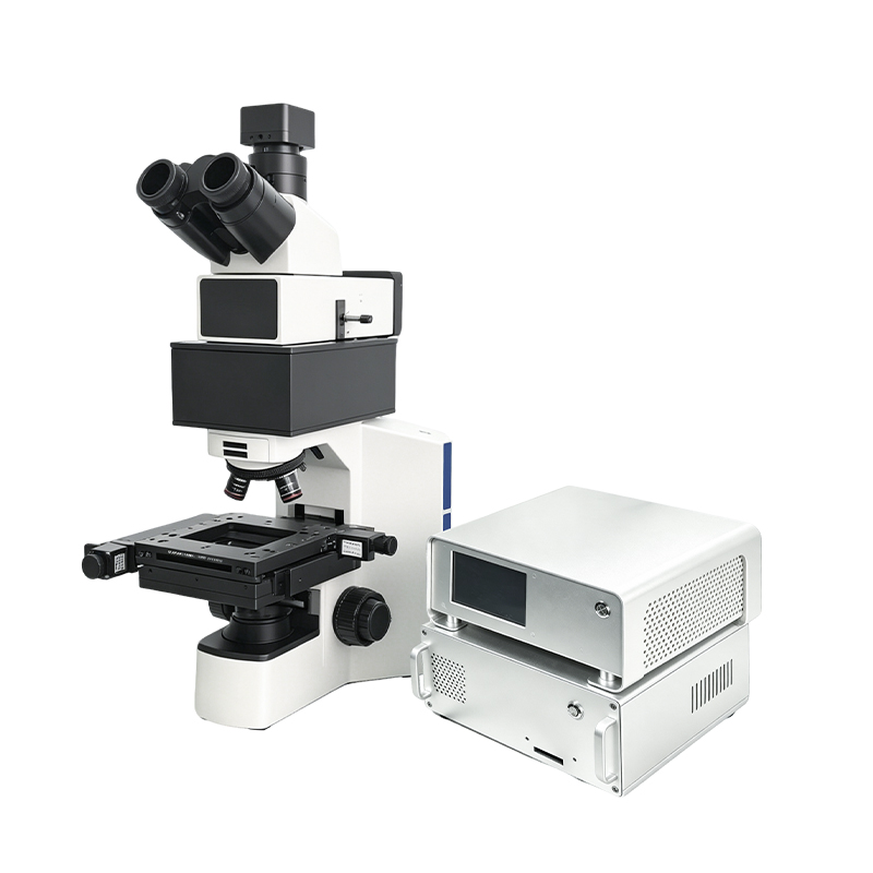
 +86 17853698681
 WhatsApp
 Product Details
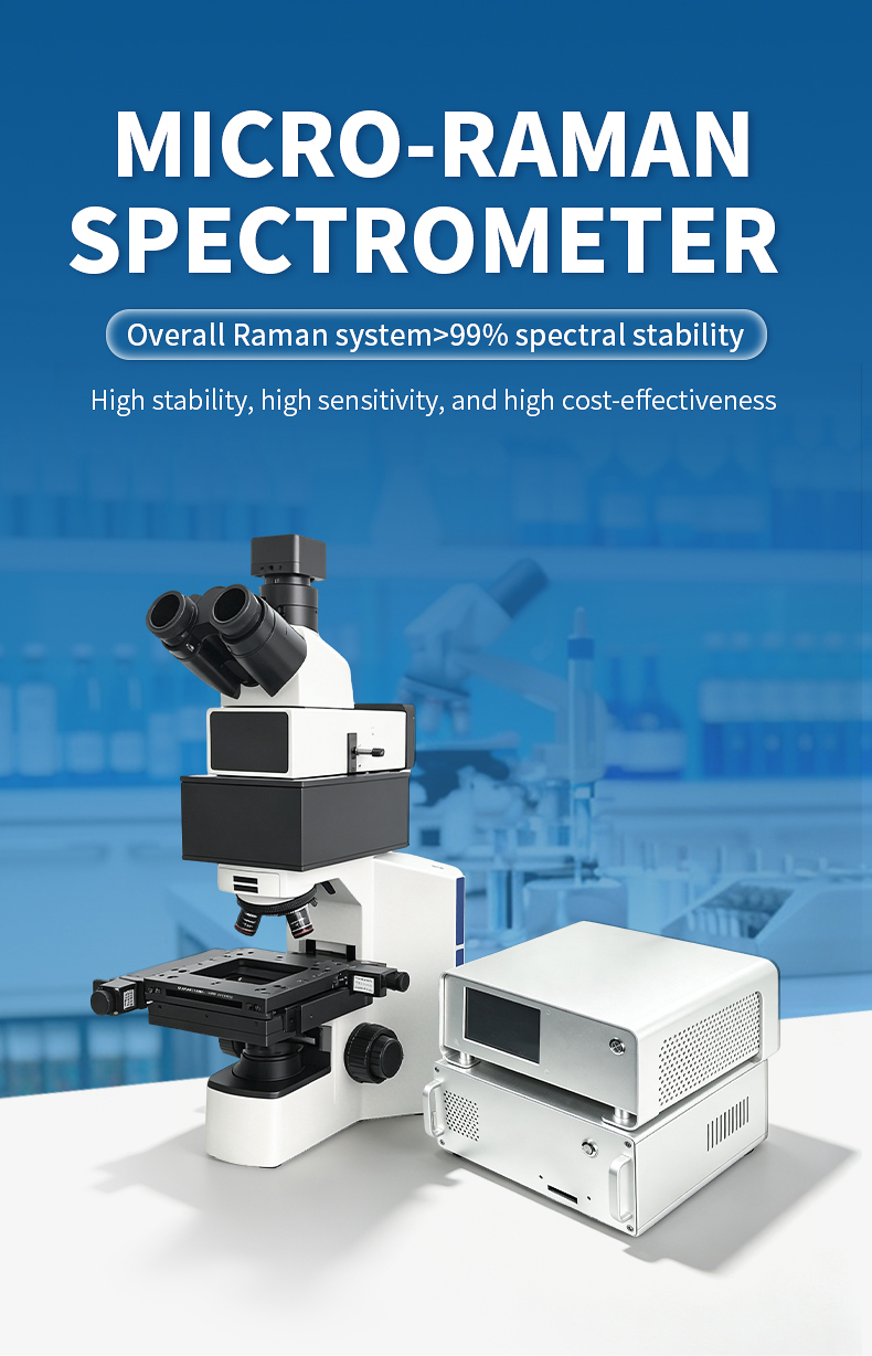


Product Introduction
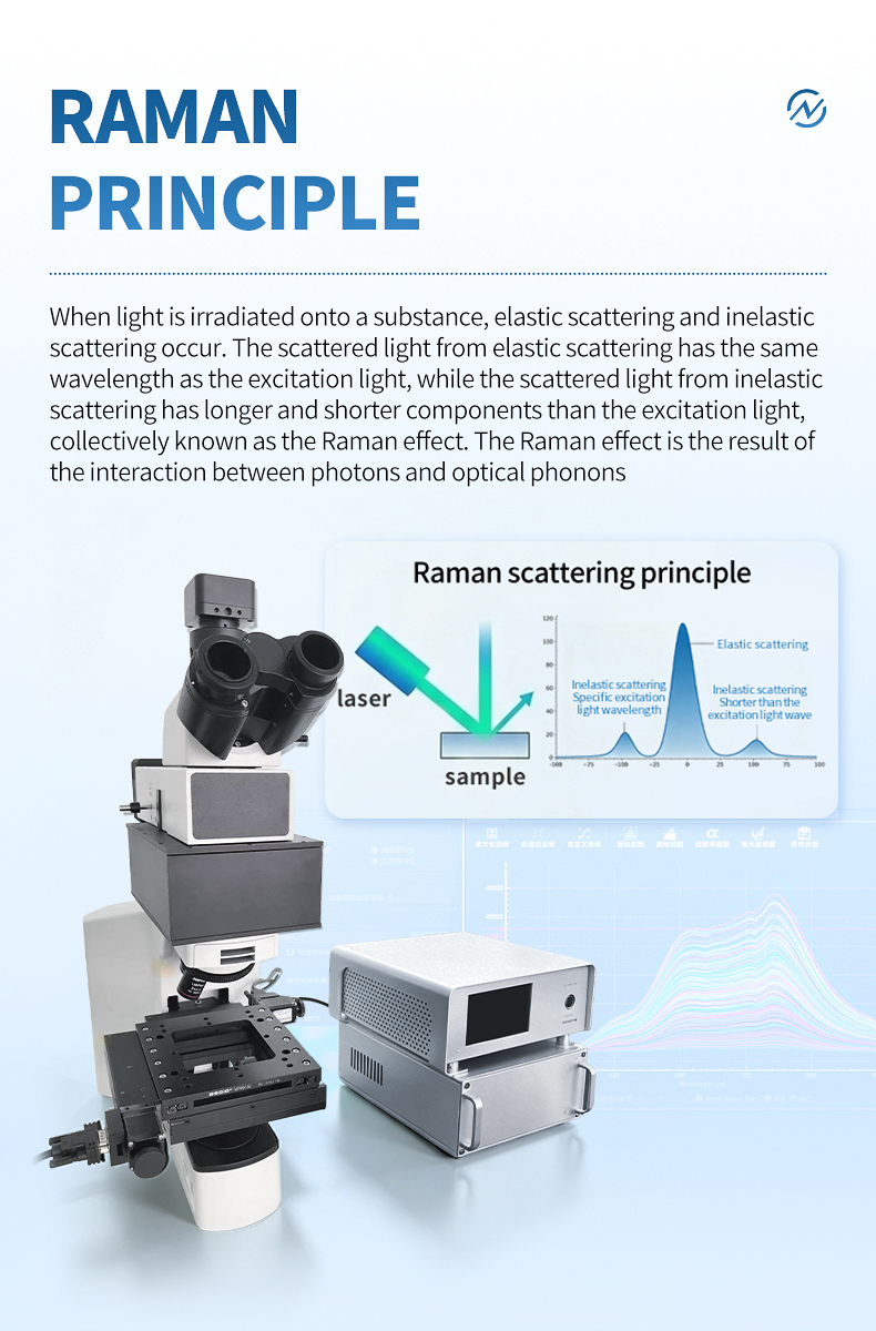
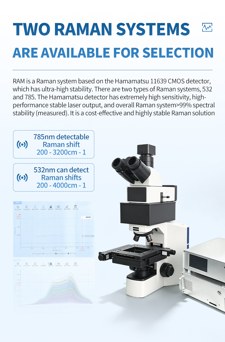
The MR-532B is HM Instruments' premium micro Raman spectrometer, purpose-built for laboratories that require automated spatial mapping capabilities alongside high-performance point analysis. Combining a 532 nm excitation laser with a precision motorized sample stage and the Hamamatsu 11639 CMOS detector, this system transforms conventional single-point Raman measurements into comprehensive two-dimensional chemical maps.
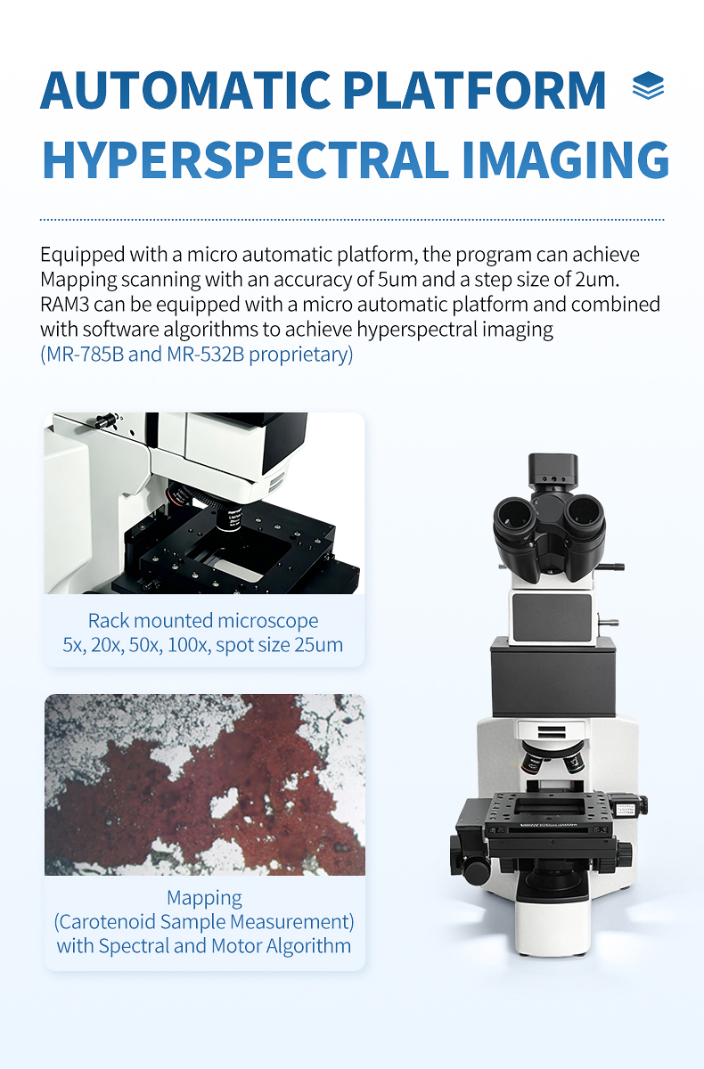
The motorized X-Y stage delivers 5 μm positioning accuracy with a minimum step size of 2 μm across a 110 mm × 75 mm travel range, enabling automated raster scanning of large sample areas without manual intervention. Integrated autofocus tracking maintains optimal focus across uneven sample surfaces, ensuring consistent spectral quality throughout extended mapping sessions. The 532 nm wavelength provides strong Raman scattering intensity, particularly advantageous for characterizing carbon nanomaterials, crystalline minerals, and inorganic compounds where fluorescence background is minimal.
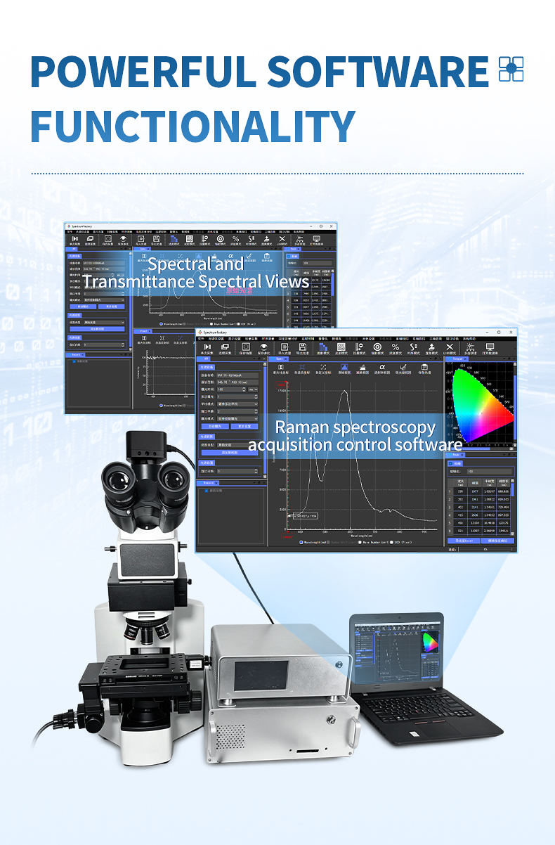
With SpectrumFactory software driving the mapping workflow — from region-of-interest definition through automated acquisition to false-color chemical image generation — the MR-532B serves as a turnkey solution for materials research, quality control laboratories, and advanced analytical facilities. For a broader market perspective, see our micro Raman spectrometer brand comparison guide.
Applications
- Hyperspectral Raman mapping of carbon nanotube and graphene film distribution across substrates
- Mineral phase mapping in thin sections for petrographic and ore deposit studies
- Active pharmaceutical ingredient (API) distribution analysis in tablet cross-sections
- Stress and strain mapping in semiconductor wafers and epitaxial layers
- Microplastic particle identification and spatial distribution on filter membranes
- Coating uniformity assessment through large-area compositional mapping
- Forensic trace evidence scanning with automated particle detection
- Art conservation pigment mapping for non-destructive cultural heritage analysis
Functional Performance and Features
- Motorized X-Y mapping stage with 5 μm positioning accuracy and 2 μm minimum step size enables high-resolution spatial chemical imaging
- 110 mm × 75 mm travel range accommodates large samples and multi-region mapping workflows without repositioning
- 532 nm excitation wavelength delivers approximately 3.5x stronger Raman signals than 785 nm for inorganic and carbon-based materials
- Hamamatsu 11639 CMOS detector with 2048 pixels and linearity exceeding 99.8% ensures quantitative spectral accuracy across the full dynamic range
- Wavenumber range of 200–4000 cm⁻¹ covers fingerprint and stretching vibration regions for comprehensive molecular characterization
- 7 cm⁻¹ spectral resolution resolves closely spaced Raman peaks in complex mineral and polymer systems
- Integrated autofocus tracking compensates for sample surface topography, maintaining consistent focal point during extended mapping runs
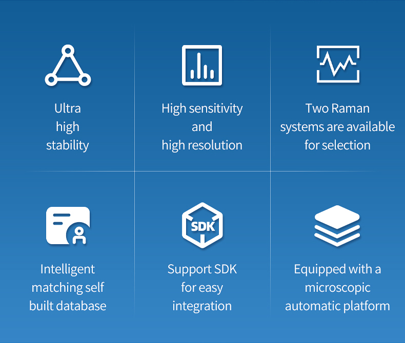
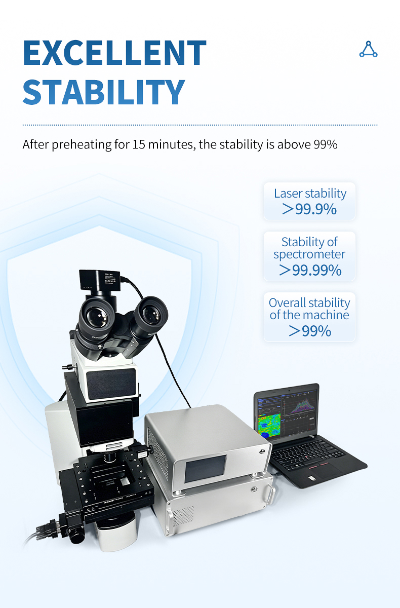
- System stability exceeding 99% over 8 hours enables unattended overnight mapping acquisitions with reliable data quality
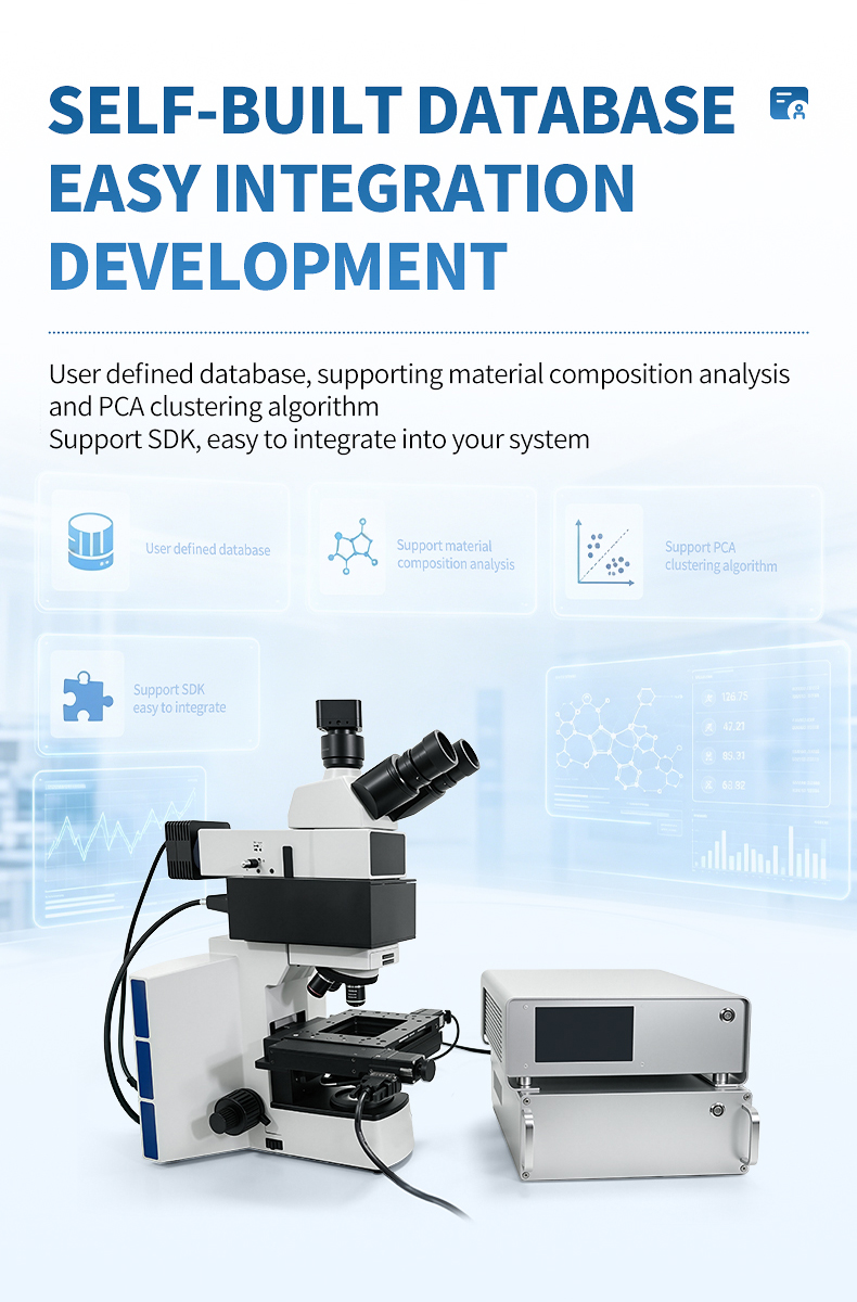
- SpectrumFactory mapping module provides region-of-interest selection, automated grid acquisition, spectral preprocessing, and false-color chemical image generation
- Signal-to-noise ratio of 500:1 with 1 ms–65 s integration time range accommodates both strong and weak scatterers in heterogeneous samples
- Rack-mounted microscope with 5x, 20x, 50x, and 100x objectives provides spot sizes down to 25 μm for micro-scale analysis
- SMA905 fiber optic interface and 4 programmable GPIO outputs support integration with external automation systems
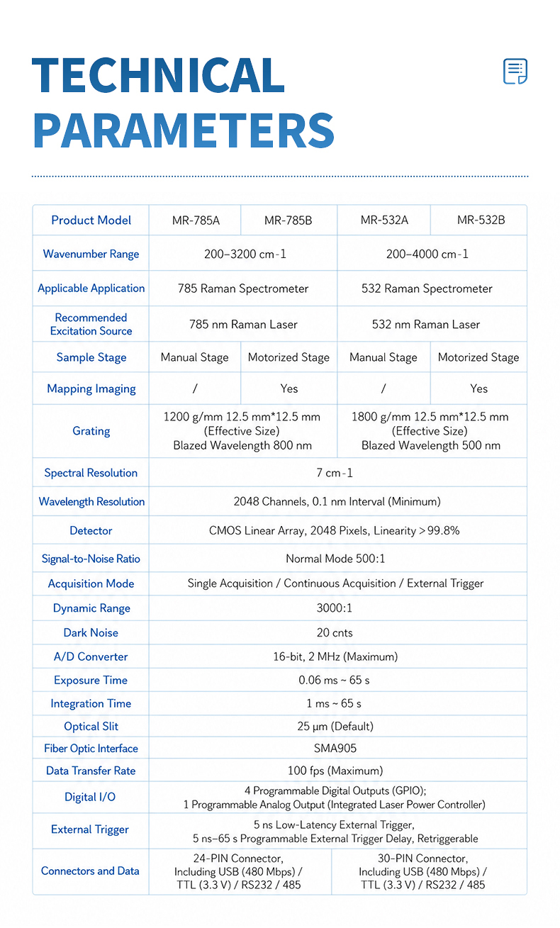
Main Parameters
| Parameter | Value |
|---|---|
| Product Model | MR-532B |
| Excitation Wavelength | 532 nm |
| Wavenumber Range | 200–4000 cm⁻¹ |
| Spectral Resolution | 7 cm⁻¹ |
| Grating | 1800 gl/mm, 12.5 mm × 12.5 mm effective size, blazed at 500 nm |
| Detector | Hamamatsu CMOS linear array, 2048 pixels, linearity > 99.8% |
| Sample Stage | Motorized mapping platform, 110 mm × 75 mm travel |
| Positioning Accuracy | 5 μm (minimum step 2 μm) |
| Microscope | Rack-mounted, 5x / 20x / 50x / 100x objectives |
| Spot Size | 25 μm |
| Reference Price | $43,000 |
Technical Parameters
| Parameter | Specification |
|---|---|
| Wavelength Resolution | 2048 channels, 0.1 nm interval (minimum) |
| Signal-to-Noise Ratio | Normal mode 500:1 |
| Acquisition Mode | Single / Continuous / External trigger / Mapping grid |
| Dynamic Range | 3000:1 |
| Dark Noise | 20 counts |
| A/D Converter | 16-bit, 2 MHz (maximum) |
| Exposure Time | 0.06 ms – 65 s |
| Integration Time | 1 ms – 65 s |
| Optical Slit | 25 μm (default) |
| Fiber Optic Interface | SMA905 |
| Data Transfer Rate | 100 fps (maximum) |
| Digital I/O | 4 programmable digital GPIO; 1 analog output (integrated laser power controller) |
| External Trigger | 5 ns low-latency, 5 ns–65 s programmable delay, retriggerable |
| Connectors | 30-pin connector, including USB (480 Mbps) / TTL (3.3 V) / RS232 / RS485 |
| Stage Travel Range | X: 110 mm, Y: 75 mm |
| Stage Positioning Accuracy | 5 μm |
| Stage Minimum Step | 2 μm |
| Autofocus | Integrated focus tracking for mapping |
| System Stability | Laser >99.9%, Spectrometer >99.99%, Overall >99% (8-hour test after 15-min warm-up) |
- Previous: MR-532A Micro Raman Spectrometer
- Next: MR-785A Micro Raman Spectrometer
 Related Products